Common Base Transistor Amplifier:
The common base transistor amplifier configuration is not as widely used as the other two formats.
Nevertheless the common base transistor amplifier finds applications where a low input impedance is required.
The common base format is probably most commonly used for RF applications, where its input impedance can be used for matching to the low source impedances often found in this arena.
Common base transistor amplifier basics:
The emitter follower transistor amplifier characteristics enable the circuit to be used as a buffer amplifier.
For both NPN and PNP circuits, it can be seen that for the common base amplifier circuit, the input is applied to the emitter, and the output is taken from the collector. The common terminal for both circuits is the base.
The common base amplifier configuration is not used as widely as transistor amplifier configurations. However it does find uses with amplifiers that require low input impedance levels. One application is for moving-coil microphones preamplifiers – these microphones have very low impedance levels. Another application is within VHF and UHF RF amplifiers where the low input impedance allows accurate matching to the feeder impedance which is typically 50Ω or 75Ω.
It is worth noting that the current gain of a common-base amplifier is always less than unity.
However the voltage gain may be more, but it is a function of input and output resistances (and also the internal resistance of the emitter-base junction). As a result, the voltage gain of a common-base amplifier can be very high.
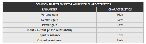
Common base transistor amplifier characteristics summary:
The table below gives a summary of the major characteristics of the common base transistor amplifier.
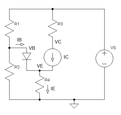
Common base transistor amplifier circuit:
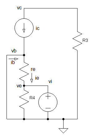
The diagram below shows how a common base amplifier circuit can be implemented.
The same bias constraints apply to the common base circuit, but the application of the signals is different, allowing the base to be earthed and hence common to both input and output circuits.
In this circuit, the same biasing conditions apply. However care has to be taken in the choice of the emitter resistor to ensure that the correct impedance match is provided for the input signal.
DC Analysis:
First we redraw the schematic using the BJT DC model. Capacitors are considered open circuit in DC and therefore are excluded.
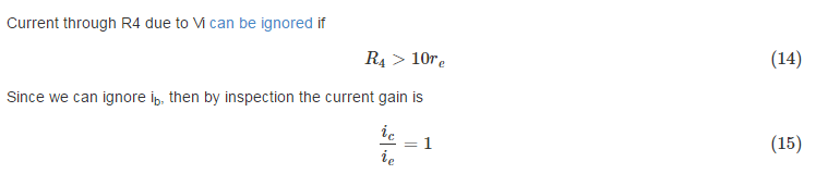
IB can be ignored if ![]()
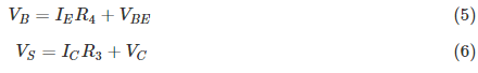
Thus VB can be calculated using KVL as simple voltage divider circuit
![]()
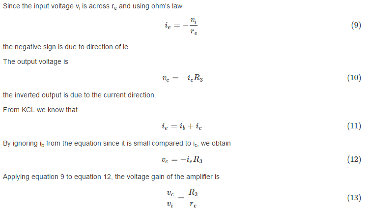
Current at Node E ![]()
if IC is much greater than IB, IB can be ignored
![]()
Using KVL (Kirchhoff’s voltage law)
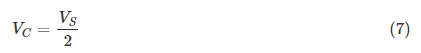
To obtain maximum output swing, you should choose the resistor values such that VC is half the supply voltage.
AC Analysis:
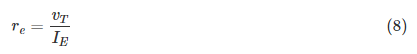
Next we redraw the schematic using the BJT small signal model. Capacitors are considered shorts in AC (R4 is shorted out by Ce) and DC supplies are connected to GND (ground). Calculate re