Bipolar Junction Transistor (BJT):
A Bipolar Junction Transistor (BJT) has three terminals connected to three doped semiconductor regions. In an N-P-N transistor, a thin and lightly doped P-type base is sandwiched between a heavily doped N-type emitter and another N-type collector; while in a P-N-P transistor, a thin and lightly doped N-type base is sandwiched between a heavily doped P-type emitter and another P-type collector. In the following, we will only consider NPN BJTs.
Bipolar Junction Transistors Characteristics:
The three parts of a BJT are collector, emitter and base. Before knowing about the bipolar junction transistor characteristics, we have to know about the modes of operation for this type of transistors. The modes are
- Common Base (CB) mode
- Common Emitter (CE) mode
- Common Collector (CC) mode
Common Collector (CC) Mode Configuration:
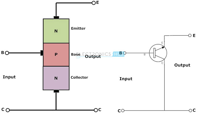
In this configuration, we use collector terminal as common for both input and output signals. This configuration is also known as emitter follower configuration because the emitter voltage follows the base voltage.
In this configuration the input signal is applied between the base-collector region and the output is taken from the emitter-collector region. Here the input parameters are VBC and IB and the output parameters are VEC and IE. The common collector configuration has high input impedance and low output impedance. The input and output signals are in phase. Here also the emitter current is equal to the sum of collector current and the base current. Now let us calculate the current gain for this configuration.
Now let us calculate the current gain for this configuration.
Current gain,
Ai = output current/Input current
Ai = IE/IB
Ai = (IC + IB)/IB
Ai = (IC/IB) + 1
Ai = β + 1
![]()
The common collector transistor circuit is shown above. This common collector configuration is a non-inverting amplifier circuit. The voltage gain for this circuit is less than unity but it has large current gain because the load resistor in this circuit receives both the collector and base currents.
Input Characteristics:
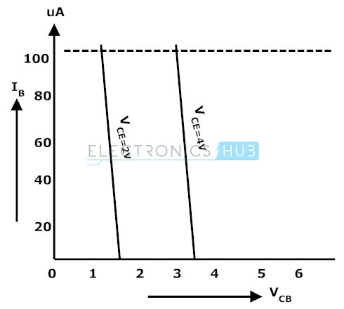
The input characteristics of a common collector configuration are quite different from the common base and common emitter configurations because the input voltage VBC is largely determined by VEC level. Here,
VEC = VEB + VBC
VEB = VEC – VBC
The input characteristics of a common-collector configuration are obtained between inputs current IB and the input voltage VCB at constant output voltage VEC. Keep the output voltage VEC constant at different levels and vary the input voltage VBC for different points and record the IB values for each point. Now using these values we need to draw a graph between the parameters of VBC and IB at constant VEC.
Output Characteristics:
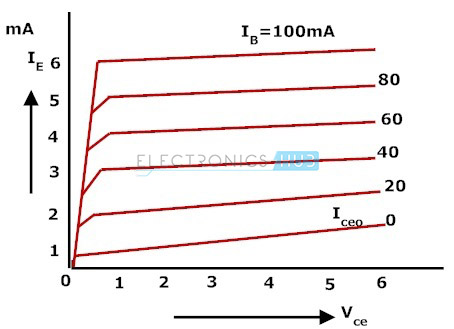
The operation of the common collector circuit is same as that of common emitter circuit. The output characteristics of a common collector circuit are obtained between the output voltage VEC and output current IE at constant input current IB. In the operation of common collector circuit if the base current is zero then the emitter current also becomes zero. As a result no current flows through the transistor
If the base current increases then the transistor operates in active region and finally reaches to saturation region. To plot the graph first we keep the IB at constant value and we will vary the VEC value for various points, now we need to record the value of IE for each point. Repeat the same process for different IB values.
Now using these values we need to plot the graph between the parameters of IE and VCE at constant values of IB. The below figure show the output characteristics of common collector.