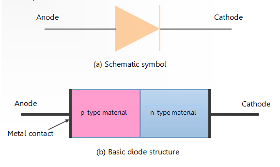
What is P-N junction:
If P-type semiconductor is joined with N-type semiconductor, a P-N junction is formed. The region in which the P-type and N-type semiconductors are joined is called P-N junction. This p-n junction separates n-type semiconductor from p-type semiconductor.
Formation of Depletion Layer:
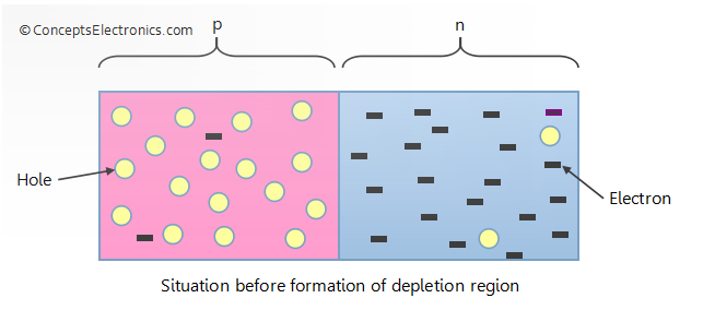
Diode is formed simply by joining p-type and n-type semiconductor material, nothing more. When P-type material is joined with n-type material, something “magical” happens which makes it one of the most widely used semiconductor device. Consider the figure below in which p-type and n-type materials are joined together.
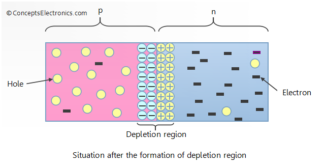
- When the two types of semiconductor materials are joined together, the electrons from the n-type material diffuse into p-type material and combines with holes.
- This creates a layer of negative ions near the junction in p-type material. Negative ions are formed because the trivalent impurities ( e.g. Aluminum) now has an extra electron from the n-type material.
- Similarly the holes from the p-type material diffuse into n-type material resulting in a layer of positive ions in the n-type material.
- These two layers of positive and negative ions form the depletion region. The term “depletion” refers to the fact that the region near the junction is depleted of their respective majority charge carriers.
The figure below shows the condition after the formation of depletion region.
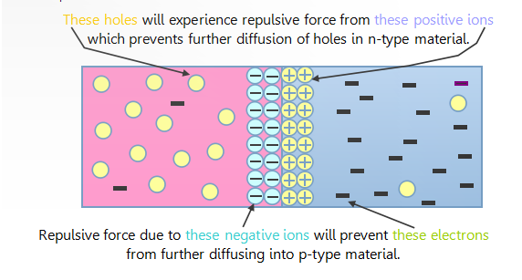
Now comes another important question- Upto what extent the diffusion of electrons and holes takes place? The diffusion does not occur indefinitely and it stops after a quick span of time and the depletion region is said to be completely formed. Take a look at the figure below to understand how this happens.
The behavior of P-N junction:
(I) Forward Biased
(II) Reverse Biased
Forward Bias:
In forward bias, the P-type is connected with the positive terminal and the n-type is connected with the negative terminal. ith a battery connected this way, the holes in the P-type region and the electrons in the N-type region are pushed toward the junction. This reduces the width of the depletion zone.
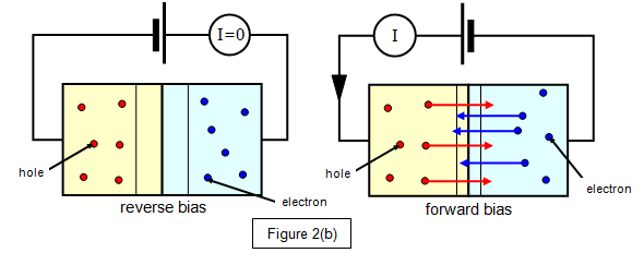
Reverse Bias:
Connecting the P-type region to the negative terminal of the battery and the N-type region to the positive terminal corresponds to reverse bias. If a diode is reverse-biased, the voltage at the cathode is comparatively higher than the anode. Therefore, no current will flow until the diode breaks down. The connections are illustrated in the diagram to the right.
