Special-Purpose Diodes:
Schottky Diodes:
Schottky diodes are constructed of a metal-to-N junction rather than a P-N semiconductor junction. Also known as hot-carrier diodes, Schottky diodes are characterized by fast switching times (low reverse recovery time), low forward voltage drop (typically 0.25 to 0.4 volts for a metal-silicon junction), and low junction capacitance.
The schematic symbol for a Schottky diode is shown in Figure below.
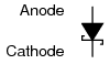
Tunnel diodes:
Tunnel diodes exploit a strange quantum phenomenon called resonant tunneling to provide a negative resistance forward-bias characteristics. When a small forward-bias voltage is applied across a tunnel diode, it begins to conduct current.
If the voltage is increased a little more, the current actually begins to decrease until it reaches a low point called the valley current (IV). If the voltage is increased further yet, the current begins to increase again, this time without decreasing into another “valley.”
The schematic symbol for the tunnel diode shown in Figure below(a).
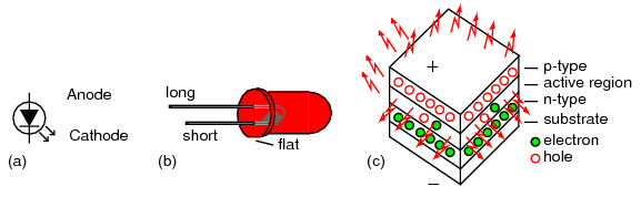
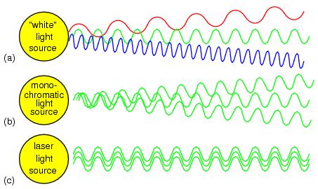
Light-emitting diodes:
Diodes, like all semiconductor devices, are governed by the principles described in quantum physics. One of these principles is the emission of specific frequency radiant energy whenever electrons fall from a higher energy level to a lower energy level.
Electrons flowing through a PN junction experience similar transitions in energy level, and emit radiant energy as they do so. The frequency of this radiant energy is determined by the crystal structure of the semiconductor material, and the elements comprising it.
Some semiconductor junctions, composed of special chemical combinations, emit radiant energy within the spectrum of visible light as the electrons change energy levels. Simply put, these junctions glow when forward biased. A diode intentionally designed to glow like a lamp is called a light-emitting diode, or LED.
Laser Diodes:
The laser diode is a further development of the regular light-emitting diode or LED. “Laser” stands for Light Amplification by Stimulated Emission of Radiation, and refers to another strange quantum process whereby characteristic light emitted by electrons falling from high-level to low-level energy states in a material stimulate other electrons in a substance to make similar “jumps,” the result being a synchronized output of light from the material.
This synchronization extends to the actual phase of the emitted light, so that all light waves emitted from a “lasing” material are not just the same frequency (color), but also the same phase as each other, so that they reinforce one another and are able to travel in a very tightly confined, nondispersive beam. This is why laser light stays so remarkably focused over long distances: each and every light wave coming from the laser is in step with each other.
Photodiodes:
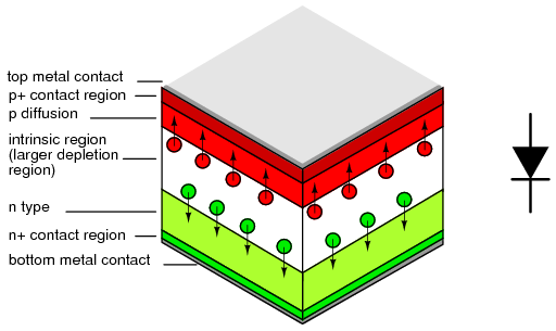
A photodiode is a diode optimized to produce an electron current flow in response to irradiation by ultraviolet, visible, or infrared light. Silicon is most often used to fabricate photodiodes; though, germanium and gallium arsenide can be used. The junction through which light enters the semiconductor must be thin enough to pass most of the light onto the active region (depletion region) where light is converted to electron-hole pairs.
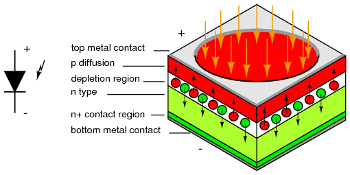
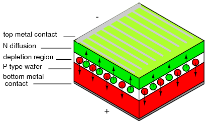
Solar Cells:
A photodiode optimized for efficiently delivering power to a load is the solar cell. It operates in photovoltaic mode (PV) because it is forward biased by the voltage developed across the load resistance.
Monocrystalline solar cells are manufactured in a process similar to semiconductor processing. This involves growing a single crystal boule from molten high purity silicon (P-type), though, not as high purity as for semiconductors. The boule is diamond sawed or wire sawed into wafers. The ends of the boule must be discarded or recycled, and silicon is lost in the saw kerf.
Since modern cells are nearly square, silicon is lost in squaring the boule. Cells may be etched to texture (roughen) the surface to help trap light within the cell. Considerable silicon is lost in producing the 10 or 15 cm square wafers.
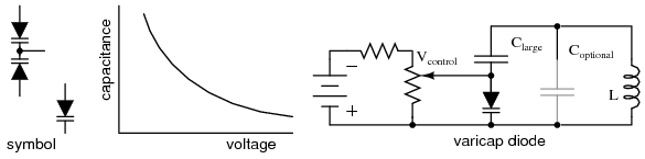
Varicap or Varactor Diodes:
A variable capacitance diode is known as a varicap diode or as a varactor. If a diode is reverse biased, an insulating depletion region forms between the two semiconductive layers. In many diodes the width of the depletion region may be changed by varying the reverse bias. This varies the capacitance. This effect is accentuated in varicap diodes.
Snap Diode:
The snap diode, also known as the step recovery diode is designed for use in high ratio frequency multipliers up to 20 gHz. When the diode is forward biased, charge is stored in the PN junction. This charge is drawn out as the diode is reverse biased. The diode looks like a low impedance current source during forward bias. When reverse bias is applied it still looks like a low impedance source until all the charge is withdrawn.
It then “snaps” to a high impedance state causing a voltage impulse, rich in harmonics. An applications is a comb generator, a generator of many harmonics. Moderate power 2x and 4x multipliers are another application.
PIN Diodes:
A PIN diode is a fast low capacitance switching diode. Do not confuse a PIN switching diode with a PIN photo diode here. A PIN diode is manufactured like a silicon switching diode with an intrinsic region added between the PN junction layers. This yields a thicker depletion region, the insulating layer at the junction of a reverse biased diode. This results in lower capacitance than a reverse biased switching diode.
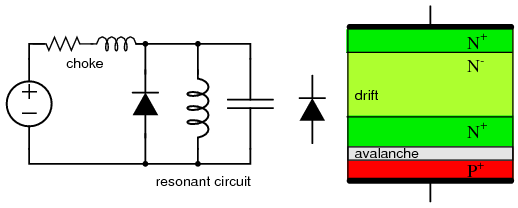
IMPATT Diode:
IMPact Avalanche Transit Time diode is a high power radio frequency (RF) generator operating from 3 to 100 gHz. IMPATT diodes are fabricated from silicon, gallium arsenide, or silicon carbide.
An IMPATT diode is reverse biased above the breakdown voltage. The high doping levels produce a thin depletion region. The resulting high electric field rapidly accelerates carriers which free other carriers in collisions with the crystal lattice. Holes are swept into the P+ region. Electrons drift toward the N regions. The cascading effect creates an avalanche current which increases even as
The cascading effect creates an avalanche current which increases even as voltage across the junction decreases. The pulses of current lag the voltage peak across the junction. A “negative resistance” effect in conjunction with a resonant circuit produces oscillations at high power levels (high for semiconductors).
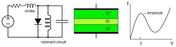
Gunn Diode:
A Gunn diode is solely composed of N-type semiconductor. As such, it is not a true diode. Figure below shows a lightly doped N– layer surrounded by heavily doped N+ layers. A voltage applied across the N-type gallium arsenide Gunn diode creates a strong electric field across the lightly doped N– layer.
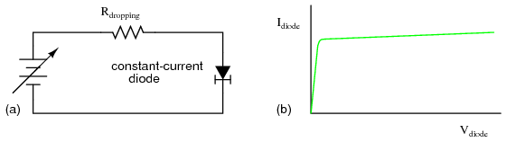
Constant-current Diodes:
A constant-current diode, also known as a current-limiting diode, or current regulating diode, does exactly what its name implies: it regulates current through it to some maximum level. The constant current diode is a two terminal version of a JFET. If we try to force more current through a constant-current diode than its current-regulation point, it simply “fights back” by dropping more voltage.