What is Tunnel diode?
Tunnel diode is a highly doped semiconductor device and is used mainly for low-voltage high-frequency switching applications. It works on the principle of Tunneling effect. It is also called as Esaki diode named after Leo Esaki, who in 1973 received the Nobel Prize in Physics for discovering the electron tunneling effect used in these diodes.
Circuit symbol:
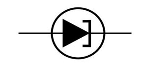
The tunnel diode is a two terminal device with p-type semiconductor acting as anode and n-type semiconductor as cathode. The circuit symbol of tunnel diode is shown.
Tunnel diode working principle:
According to the classical laws of physics, a charged particle sin order to cross an energy barrier should possess energy at least equal to the energy barrier. Hence the particle will cross the energy barrier if its energy is greater than the barrier and cannot cross the barrier if its energy is less than the energy barrier.
But quantum mechanically there exists non zero probability that the particle with energy less than the energy barrier will cross the barrier as if it tunnels across the barrier. This is called as Tunneling effect. The probability increases with the decreasing barrier energy.
P α exp (-A*Eb *W)
Where P is the probability that the particle crosses the barrier,
Eb is the barrier energy
W is the barrier width.
In normal PN junction diodes the doping levels will be of the order 1 dopant atom in 108 atoms of Si (or) Ge. If the doping levels are increased to 1 in 103, the depletion layer width is of the order of 10 nm. In such a PN junction tunneling effect is significant, such PN junction devices are called Tunnel diodes.
V-I characteristics of Tunnel diode:
The IV characteristics of the tunnel diode is shown below
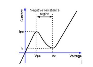
For small forward voltages owing to high carrier concentrations in tunnel diode and due to tunneling effect the forward resistance will be very small. As voltage increase she current also increases till the current reaches Peak current.
If the voltage applied to tunnel diode is increased beyond the peak voltage the current will start decreasing. This is negative resistance region. It prevails till valley point. At valley point the current through the diode will be minimum. Beyond valley point the tunnel diode acts as normal diode. In reverse biased condition also Tunnel diode is an excellent conductor due to its high doping concentrations.
Tunnel diodes are made from Germanium or gallium arsenide due to their highest peak voltage to valley point swing. The ratio of high peak current to valley current quantifies the maximum voltage swing allowed in negative resistance region.
Current components in a tunnel diode:
The total current in a tunnel diode is given as It = Itun + Idiode + Iexcess. The diode current in a tunnel diode is same as that for normal PN junction diode which is given as
Idiode = Ido*(exp (V/ (η *Vt))-1)
Where Ido is reverse saturation current and will be very high in tunnel diode compared to PN junction diode due to high doping concentrations,
V is voltage applied across diode,
Vt is the voltage equivalent of temperature,
η is correction factor 1 for Ge and 2 for Si,
For Voltages less than the cut-in voltage of the diode this current is negligible.
The excess current is an additional current due to parasitic tunneling via impurities which determines the valley point. The tunneling current in given as
Itun = (V/Ro)*exp (-(V/Vo)m)
Where m= 1 to 3 and VO = 0.1 to 0.5 volts, RO is the tunnel diode resistance.
Peak voltage, Peak current of tunnel diode:
The peak voltage of a tunnel diode can be found as follows: At peak voltage current through the tunnel diode is maximum. Typically the peak voltage will be less than cut in voltage of tunnel diode and hence the diode current and excess current can be considered negligible.
Hence for maximum or minimum diode current
V=Vpeak, dItun/dV = 0
which is
(1/Ro)*(exp (-(V/Vo)m)-(m*(V/Vo)m*exp(-(V/Vo)m) = 0 and
This implies 1- m*(V/Vo)
1- m*(V/Vo)m = 0 and
Vpeak = ((1/m)(1/m))*Vo , Ipeak = ((1/m)(1/m))*Vo*exp(-1/m).
Maximum negative resistance of tunnel diode:
The small signal negative resistance is given as
Rn = 1/(dI/dV) = RO/(1-(m*(V/Vo)m)* exp(-(V/Vo)m).
When Rn is maximum dI/dV = 0, so (1-(m*(V/Vo)m)* exp(-(V/Vo)m)/Ro = 0
Hence at V = Vo*(1+1/m)(1/m) |Rn| is maximum hence (Rn)max = -(RO*(exp(1+m)/m))/m
Small signal model of tunnel diode:
The small signal model of tunnel diode in negative resistance region is shown below
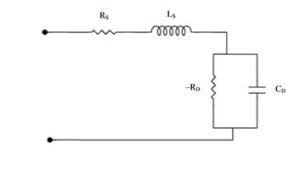
Where the resistance Rs is Ohmic resistance
-Rn is slope of VI characteristics in negative resistance region = 1/(dI/dV)
Ls is series inductance due to metal leads
C is junction capacitance = (ε*A/W)
ε is the permittivity of depletion region
Advantages of tunnel diode:
- High speed of operation due to the fact that the tunneling takes place at the speed of light.
- Low cost
- Low noise
- Environmental immunity
- Low power dissipation
- Simplicity in fabrication
- Longevity
Disadvantages of tunnel diode:
- Low output voltage swing
- Because it is a two terminal device, there is no isolation between input and output.
Applications of tunnel diode:
Some of the applications of Tunnel diode are
- Tunnel diodes are used as very high-speed switches.
- Used as high-frequency micro wave oscillator.
