Common Collector Transistor Amplifier:-
A Common Collector Amplifier is formed from the basic Bipolar Junction transistor. Basically it is required to have four terminals so that two are preferred for the input and the remaining two is for output side. But it has only three terminals named as collector, base and the emitter. Among these terminals one is made common so that it can be connected on both sides of input as well as output. The configuration of the common collector is also known as emitter follower because of its dependence on emitter terminal and its currents.
What is CC Amplifier?
An amplifier circuitry which is designed by considering the collector terminal to be common for the input and the output sides is defined as Common Collector Amplifier. It is highly known for its feature of producing higher values of the gain in current.
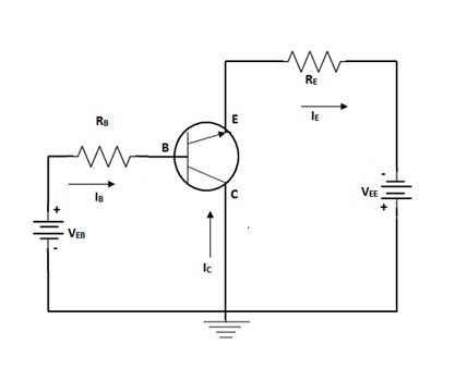
Common Collector Circuit Diagram
Common Collector Amplifier Design/Working
The basic purpose of the amplifier is to amplify the signals and that improvises the strength of the signal. The input is to be applied at the base terminal. The collector is to be treated common for both input and the output sides or sometimes considered to be grounded.
The current at the output is to be taken from the emitter. Hence the load receives the currents from the base and the emitter. The emitter current generated is the sum of the base and the collector currents. This results in the increase amount of current and the gain value of the current is maximum in this case. The input value of the voltage and the output value of the voltage generated are in direct relation with each other. Hence there is no phase shifts are evident in between the applied input and the output signals generated.
Based on the resistors connected at the respective terminals it is responsible for maintaining the quiescent point in the active region. Hence the transistor behaves efficiently in such cases and acts as an amplifier results in the increase of the signal strength. But it is unable to match the requirements so that its design can be considered to be having large amounts in current gain because of its ups and downs in the input impedance values. In order to overcome this pair of this common collector configure transistors are connected.
| COMMON COLLECTOR, EMITTER FOLLOWER TRANSISTOR AMPLIFIER CHARACTERISTICS | |||
|---|---|---|---|
| PARAMETER | CHARACTERISTICS | ||
| Current gain | High | ||
| Voltage gain | Zero | ||
| Power gain | Medium | ||
| Input / output phase relationship | 0° | ||
| Input resistance | High | ||
| Output resistance | Low | ||
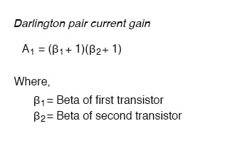
The drawback of the emitter follower can be overcome by connecting them in pairs. The pairs are connected in such a way that the output of the transistor is connected to the input of the base of the second transistor. The efficiency of the transistor is increased due to the Darlington pair configuration.
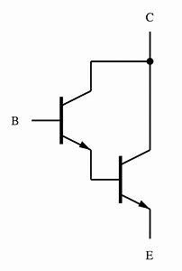
Symbol of Darlington Transistor Pair Configuration of Common Collector Configuration
Characteristics
The basic characteristics of the common collector amplifier are as follows.
- The variation in between the applied input and the output voltage is directly related to each other. That is increase in the input voltage also makes the output voltage to increase. Practically if there simulation results are noted there will be only 0.7 volts difference between the signals generated at the output because of the input.
- As the circuit of this configuration is designed its input is taken across base and the output is across the emitter.
- In this type of amplifier the load resistance is able to receive the currents from both the emitter and the base terminals.
- The resultant emitter current is the combination of the base and the collector currents. This makes the circuit to achieve the higher current gains.
- It maintains the gain of the voltage at the level of unity.
- The gain of power for this transistor is to be at medium.
- There is no evident phase shift between applied input and the generated output signals.
- The resistance at the input of this circuit is high enough.
- The resistance value at the output for this circuit is considered to be low.
The above discussed are the some of the characteristics of the common collector amplifier.
Applications of Common Collector Amplifier
The common collector has the great applications because of its high current gains. It is also known for its direct relation between the applied input and the output voltages. Some of the applications are listed as follows.
- In the matching circuitry of impedance these circuits are utilized.
- It is well known for its capability of switching technique.
- For the buffering applications these transistors are used.
- In the isolation of the circuits these transistors are used.
Since the common collector current gain is defined as the ratio of the emitter current to the base current, γ = IE/IB = β + 1, it therefore follows that the amplifiers current gain must be approximately equal to Beta (β) as β + 1 is virtually the same as Beta
