Bipolar Junction Transistor (BJT):
A Bipolar Junction Transistor (BJT) has three terminals connected to three doped semiconductor regions. In an N-P-N transistor, a thin and lightly doped P-type base is sandwiched between a heavily doped N-type emitter and another N-type collector; while in a P-N-P transistor, a thin and lightly doped N-type base is sandwiched between a heavily doped P-type emitter and another P-type collector. In the following, we will only consider NPN BJTs.
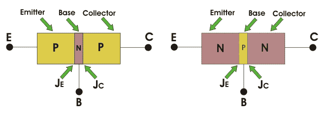
Bipolar Junction Transistors Characteristics:
The three parts of a BJT are collector, emitter and base. Before knowing about the bipolar junction transistor characteristics, we have to know about the modes of operation for this type of transistors. The modes are
- Common Base (CB) mode
- Common Emitter (CE) mode
- Common Collector (CC) mode
Common-Emitter (CE) mode Characteristics:
In this configuration, we use emitter as common terminal for both input and output. This common emitter configuration is an inverting amplifier circuit. Here the input is applied between base-emitter region and the output is taken between collector and emitter terminals. In this configuration the input parameters are VBE and IB and the output parameters are VCEand IC.
This type of configuration is mostly used in the applications of transistor based amplifiers. In this configuration the emitter current is equal to the sum of small base current and the large collector current. i.e. IE = IC + IB. We know that the ratio between collector current and emitter current gives current gain alpha in Common Base configuration
We know that the ratio between collector current and emitter current gives current gain alpha in Common Base configuration similarly the ratio between collector current and base current gives the current gain beta in common emitter configuration.
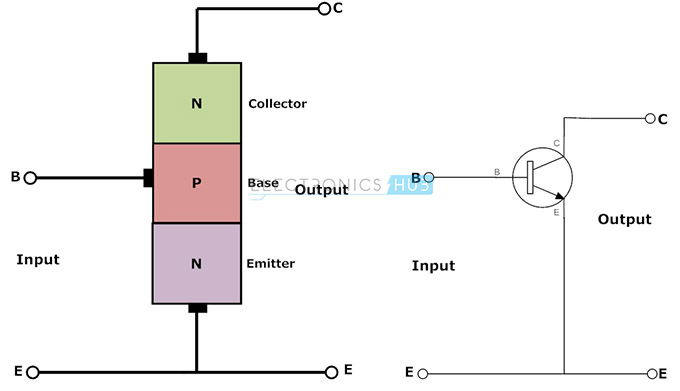
Now let us see the relationship between these two current gains.
Current gain (α) = IC/IE
Current gain (β) = IC/IB
Collector current IC =α IE = βIB
This configuration is mostly used one among all the three configurations. It has medium input and output impedance values. It also has the medium current and voltage gains. But the output signal has a phase shift of 1800 i.e. both the input and output are inverse to each other.
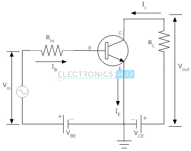
Input Characteristics:
Input characteristics IB (Base Current) is the input current, VBE (Base – Emitter Voltage) is the input voltage for CE (Common Emitter) mode. So, the input characteristics for CE mode will be the relation between IB and VBE with VCE as parameter. The characteristics are shown below
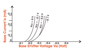
The typical CE input characteristics are similar to that of a forward biased of p – n diode. But as VCB increases the base width decreases.
Output Characteristics:
Output Characteristics Output characteristics for CE mode is the curve or graph between collector current (IC) and collector – emitter voltage (VCE) when the base current IB is the parameter. The characteristics is shown below in the figure.
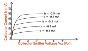
Like the output characteristics of common – base transistor CE mode has also three regions named-
(i) Active region,
(ii) cut-off regions,
(iii) saturation region.
The active region has collector region reverse biased and the emitter junction forward biased. For cut-off region, the emitter junction is slightly reverse biased and the collector current is not totally cut-off. And finally for saturation region both the collector and the emitter junction are forward biased.
