Inverting Operational Amplifier:
– the inverting amplifier using an op-amp is one of the most widely used operational amplifier circuits especially as it can be used as a summing amplifier or virtual earth mixer.
Basic inverting amplifier circuit:
The basic circuit for the inverting op amp circuit is shown below. It consists of a resistor from the input terminal to the inverting amplifier input of the circuit, and another resistor connected from the output to the inverting input of the op-amp. The non-inverting input is connected to ground.
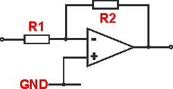
In this inverting amplifier circuit the non-inverting input of the operational amplifier is connected to ground. As the gain of the op amp itself is very high and the output from the amplifier is a matter of only a few volts, this means that the difference between the two input terminals is exceedingly small and can be ignored. As the non-inverting input of the operational amplifier is held at ground potential this means that the inverting input must be virtually at earth potential. As a result, this form of amplifier is often known as a virtual earth amplifier.
Inverting Operational Amplifier Configuration:
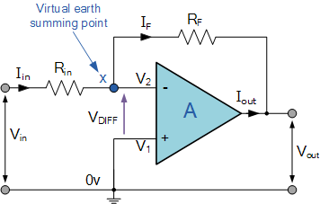
In this Inverting Amplifier circuit the operational amplifier is connected with feedback to produce a closed loop operation. When dealing with operational amplifiers there are two very important rules to remember about inverting amplifiers, these are: “No current flows into the input terminal” and that “V1 always equals V2”. However, in real world op-amp circuits both of these rules are slightly broken.
This is because the junction of the input and feedback signal ( X ) is at the same potential as the positive ( + ) input which is at zero volts or ground then, the junction is a “Virtual Earth”. Because of this virtual earth node the input resistance of the amplifier is equal to the value of the input resistor, Rin and the closed loop gain of the inverting amplifier can be set by the ratio of the two external resistors.
We said above that there are two very important rules to remember about Inverting Amplifiers or any operational amplifier for that matter and these are.
- No Current Flows into the Input Terminals
- The Differential Input Voltage is Zero as V1 = V2 = 0 (Virtual Earth)
Then by using these two rules we can derive the equation for calculating the closed-loop gain of an inverting amplifier, using first principles.
Current ( i ) flows through the resistor network as shown.
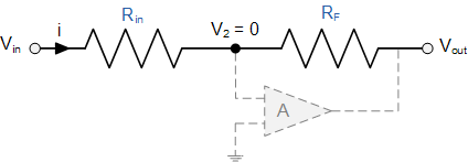
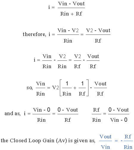
Then, the Closed-Loop Voltage Gain of an Inverting Amplifier is given as.

and this can be transposed to give Vout as:

The negative sign in the equation indicates an inversion of the output signal with respect to the input as it is 180o out of phase. This is due to the feedback being negative in value.

The equation for the output voltage Vout also shows that the circuit is linear in nature for a fixed amplifier gain as Vout = Vin x Gain. This property can be very useful for converting a smaller sensor signal to a much larger voltage.
Another useful application of an inverting amplifier is that of a “transresistance amplifier” circuit. A Transresistance Amplifier also known as a “transimpedance amplifier”, is basically a current-to-voltage converter (Current “in” and Voltage “out”). They can be used in low-power applications to convert a very small current generated by a photo-diode or photo-detecting device etc, into a usable output voltage which is proportional to the input current as shown.
Inverting- amplifier input impedance:
One key consideration when designing an inverting amplifier is the input impedance. This governs many of the requirements in terms of coupling between stages, particularly when they are AC coupled.
The input impedance is easy to determine
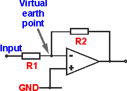
Using the diagram it is easy to determine the input impedance. As the inverting input to the amplifier is at earth potential, the input impedance is simply the value of R1.

Inverting amplifier design considerations:
There are a number of design considerations and tips to be kept in mind when designing an inverting amplifier circuit using an op amp.
- Bandwidth product: It is worth mentioning at this point that for high levels of gain, the gain bandwidth product of the basic op amp itself may become a problem. With levels of gain of 100, the bandwidth of some operational amplifier ICs may only be around 3 kHz. Check the data sheet for the given chip being used before settling on the level of gain.
- Input impedance: With the value of R1, the input resistor being lower than the feedback resistor R2, care has to be taken when designing he circuit to ensure the input resistance is not too low for any given application. Often values of 10kΩ are used as this provides a reasonable load resistance for many circuits. However the exact requirements need to be determined for each application.
- Range of values for R1 and R2: When designing an inverting amplifier it is necessary to ensure that the values of the resistor used remain within ‘sensible’ bounds. If the input resistor is made too low, then the circuit may load the previous circuit too much. If high gain levels are required, then this may mean that the feedback resistor, R2 must be higher. Even though the input impedance of the integrated circuit itself circuit may be high, using a high value of feedback resistor is not advisable as results may become a little unpredictable. As a very broad rule of thumb values for R2 of up to 100kΩ or a little more should be fine. Values above this should be used with a little caution, as the circuit may produce some unexpected effects, although in many instances they may work acceptably well.
Summing amplifier / virtual earth mixer:
The fact that the inverting input to the amplifier is virtually at earth potential provides some significant possibilities for audio mixer applications.
This form of virtual earth mixer, or summing amplifier adds several different signals in a linear or additive fashion. It is not the form of multiplier mixer used in RF circuits where a non-linear action is used.
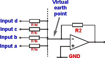
There is almost no limit to the number of inputs that can be added. The gain for each leg being R2 / R1y where R1 y is the input resistor for that particular channel.
