Transistor Biasing:
The basic function of transistor is amplification. The process of raising the strength of weak signal without any change in its general shape is referred as faithful amplification. For faithful amplification it is essential that:-
- Emitter-Base junction is forward biased
- Collector- Base junction is reversed biased
- Proper zero signal collector current
WHY BIASING?
If the transistor is not biased properly, it would work inefficiently and produce distortion in output signal.
BIAS STABILITY:
Through proper biasing, a desired quiescent operating point of the transistor amplifier in the active region (linear region) of the characteristics is obtained. It is desired that once selected the operating point should remain stable. The maintenance of operating point stable is called Stabilisation.
The selection of a proper quiescent point generally depends on the following factors:
- The amplitude of the signal to be handled by the amplifier and distortion level in signal.
- The load to which the amplifier is to work for a corresponding supply voltage.
The operating point of a transistor amplifier shifts mainly with changes in temperature, since the transistor parameters —
(where the symbols carry their usual meaning)—are functions of temperature.
The DC Operating Point:
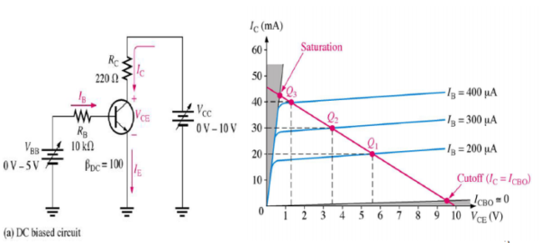
For a transistor circuit to amplify it must be properly biased with dc voltages. The dc operating point between saturation and cutoff is called the Q-point. The goal is to set the Q-point such that that it does not go into saturation or cutoff when an a ac signal is applied.

Requirements of biasing network:
- Ensuring proper zero signal collector current.
- Ensuring Vce not falling below 0.5V for Ge transistor and 1V for Silicon transistor at any instant.
- Ensuring Stabilization of operating point
![]()
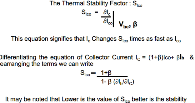
The Thermal Stability of Operating Point (SIco):
Stability Factor S:-
The stability factor S, as the change of collector current with respect to the reverse saturation current, keeping
β and VBE constant. This can be written as:

