What is a Zener Diode?
A Zener Diode or “Breakdown Diode”, are basically the same as the standard PN junction diode but they are specially designed to have a low and specified Reverse Breakdown Voltage which takes advantage of any reverse voltage applied to it.
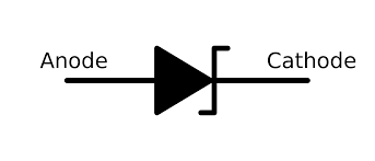
Symbol
However, as soon as the reverse voltage reaches a pre-determined value, the zener diode begins to conduct in the reverse direction. This is because when the reverse voltage applied across the zener diode exceeds the rated voltage of the device a process called Avalanche Breakdown occurs in the semiconductor depletion layer and a current starts to flow through the diode to limit this increase in voltage.
The current now flowing through the zener diode increases dramatically to the maximum circuit value and once achieved, this reverse saturation current remains fairly constant over a wide range of reverse voltages. The voltage point at which the voltage across the zener diode becomes stable is called the “zener voltage”, ( Vz ) and for zener diodes this voltage can range from less than one volt to a few hundred volts.
The point at which the zener voltage triggers the current to flow through the diode can be very accurately controlled in the doping stage of the diodes semiconductor construction giving the diode a specific zener breakdown voltage, ( Vz ) for example, 4.3V or 7.5V. This zener breakdown voltage on the I-V curve is almost a vertical straight line.
Zener Diode I-V Characteristics

The Zener Diode is used in its “reverse bias” or reverse breakdown mode, i.e. the diodes anode connects to the negative supply. From the I-V characteristics curve above, we can see that the zener diode has a region in its reverse bias characteristics of almost a constant negative voltage regardless of the value of the current flowing through the diode.
This voltage remains almost constant even with large changes in current providing the zener diodes current remains between the breakdown current IZ(min) and its maximum current rating IZ(max).
This ability of the zener diode to control itself can be used to great effect to regulate or stabilize a voltage source against supply or load variations.
The function of a voltage regulator is to provide a constant output voltage to a load connected in parallel with it in spite of the ripples in the supply voltage or variations in the load current. A zener diode will continue to regulate its voltage until the diodes holding current falls below the minimum IZ(min) value in the reverse breakdown region.
The Zener Diode as Voltage Regulator
Zener Diodes can be used to produce a stabilized voltage output with low ripple under varying load current conditions. By passing a small current through the diode from a voltage source, via a suitable current limiting resistor (RS), the zener diode will conduct sufficient current to maintain a voltage drop of Vout. By connecting a simple zener stabilizer circuit as shown below across the output of the rectifier, a more stable output voltage can be produced.
Zener Diode Regulator

Resistor, RS is connected in series with the zener diode to limit the current flow through the diode with the voltage source, VS being connected across the combination. The stabilized output voltage Vout is taken from across the zener diode.
The zener diode is connected with its cathode terminal connected to the positive rail of the DC supply so it is reverse biased and will be operating in its breakdown condition. Resistor RS is selected so to limit the maximum current flowing in the circuit.
With no load connected to the circuit, the load current will be zero, ( IL = 0 ), and all the circuit current passes through the zener diode which in turn dissipates its maximum power. Also a small value of the series resistor RS will result in a greater diode current when the load resistance RL is connected and large as this will increase the power dissipation requirement of the diode so care must be taken when selecting the appropriate value of series resistance so that the zener’s maximum power rating is not exceeded under this no-load or high-impedance condition.
The load is connected in parallel with the zener diode, so the voltage across RL is always the same as the zener voltage, ( VR = VZ ). There is a minimum zener current for which the stabilization of the voltage is effective and the zener current must stay above this value operating under load within its breakdown region at all times. The upper limit of current is of course dependent upon the power rating of the device. The supply voltage VS must be greater than VZ.
One small problem with zener diode stabilizer circuits is that the diode can sometimes generate electrical noise on top of the DC supply as it tries to stabilize the voltage. Normally this is not a problem for most applications but the addition of a large value decoupling capacitor across the zener’s output may be required to give additional smoothing.
Then to summarize a little, a zener diode is always operated in its reverse biased condition. As such a simple voltage regulator circuit can be designed using a zener diode to maintain a constant DC output voltage across the load in spite of variations in the input voltage or changes in the load current.
The zener voltage regulator consists of a current limiting resistor RS connected in series with the input voltage VS with the zener diode connected in parallel with the load RL in this reverse biased condition. The stabilized output voltage is always selected to be the same as the breakdown voltage VZ of the diode.
Zener Diode Voltages
As well as producing a single stabilized voltage output, zener diodes can also be connected together in series along with normal silicon signal diodes to produce a variety of different reference voltage output values as shown below.
Zener Diodes Connected in Series

The values of the individual Zener diodes can be chosen to suit the application while the silicon diode will always drop about 0.6 – 0.7V in the forward bias condition. The supply voltage, Vin must of course be higher than the largest output reference voltage and in our example above this is 19v.
Zener Diode Clipping Circuits
Diode clipping and clamping circuits are circuits that are used to shape or modify an input AC waveform (or any sinusoidal) producing a differently shape output waveform depending on the circuit arrangement. Diode clipper circuits are also called limiters because they limit or clip-off the positive (or negative) part of an input AC signal. As zener clipper circuits limit or cut-off part of the waveform across them, they are mainly used for circuit protection or in waveform shaping circuits.
Square Wave Signal

So for example, if we wanted to clip an output waveform between two different minimum and maximum values of say, +8V and -6V, we would simply use two differently rated zener diodes. Note that the output will actually clip the AC waveform between +8.7V and -6.7V due to the addition of the forward biasing diode voltage.
In other words a peak-to-peak voltage of 15.4 volts instead of expected 14 volts, as the forward bias volt drop across the diode adds another 0.7 volts in each direction.
This type of clipper configuration is fairly common for protecting an electronic circuit from over voltage. The two zener’s are generally placed across the power supply input terminals and during normal operation, one of the zener diodes is “OFF” and the diodes have little or no affect. However, if the input voltage waveform exceeds its limit, then the zener’s turn “ON” and clip the input to protect the circuit.
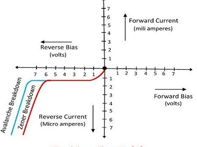
Breakdown Characteristic Graph
The graphical representation of the Avalanche and Zener breakdown is shown in the figure below.
Definition of Avalanche Breakdown
The avalanche breakdown is the breakdown mechanism of the PN – junction diodes which have thinner region. In this breakdown, when the electric field is applied across the diode, the velocity of the charge carrier increases. This charge carrier collides with the other atoms and creates the pairs of hole and electrons.
The free charge carrier further collides with other atoms and creates more pairs of electron and hole. These free electrons start moving across the junction and develop the reverse bias current. The reverse bias current completely destroys the junction. And once the junction breakdown occurs, it cannot regain its original position.
Definition of Zener Breakdown
The junction breakdown mechanism which occurs in the heavily doped thin region is called Zener breakdown. In this mechanism when the high electric field is applied across the junction, the charge carrier starts jumping across the junction. These electrons constitute the heavy current in the reversed direction. In Zener breakdown, the temporary breakdown of junction occurs. The junction regains its original position when the reverse voltage removes.


