Break Down Mechanism in P-N Junction Diode:
If the reverse-bias applied to a p-n junction is increased, a point will reach when the junction breaks down and reverse current rises sharply to a value limited only by the external resistance connected in series. This specific value of the reverse bias voltage is called breakdown voltage (vz). After breakdown, a very small further increase the reverse current. The breakdown voltage depends upon the width of depletion layer. The width of depletion layer depends upon the doping level.
The following two processes cause junction breakdown due to the increase in reverse bias voltage.
(i) Zener Breakdown
(ii) Avalanche Breakdown
Zener Breakdown:
The Zener breakdown takes place in a very thin junction, i.e., the depletion layer is narrow when both the sides of the junction are very heavily doped. In the Zener breakdown mechanism, the electric field becomes as high as 107 V/m in the depletion layer with only a small applied reverse bias voltage.
In this process, it became possible for some of the electrons to jump across the barrier from the valence band in p material to some of the unfilled conduction band in n material. This process is known as Zener Breakdown. In this process, the junction is not damaged. The junction regains its original position when the reverse voltage is removed. This process is used in the Zener diode.
However, if the number of electrons jumping across the barrier (i.e., the flow of current) increases beyond the rated capacity of the Zener diode, then Avalanche breakdown takes place which destroys the junction.
A current limiting resistance should be connected in series with the Zener diode to protect it against the damage due to excessive heating. In Zener breakdown, the breakdown voltage depends on the temperature of P-N junction.The breakdown voltage decreases with increase in the junction temperature.
Avalanche Breakdown:
For thicker junctions, the breakdown mechanism is by the process of Avalanche breakdown. In this mechanism, when the electric field existing in the depletion layer is sufficiently high, the velocity of the carriers (minority carriers) crossing the depletion layer increases. These carriers (electrons and holes) collide with the crystal atoms. Some collisions are so violent that the electrons are knocked off the crystal tom thus creating electron-hole pairs.
As the pair of electron hole is created in the midst of the high field, they quickly separate and attain high velocities to cause further pair generation through more collision. It is a cumulative process and it goes on. As the breakdown voltage is going to achieve the field becomes so large that the chain of collisions can give rise to an almost infinite current with a very slight additional increase in the voltage.
Due to this additionally acquired energy, these valence electrons will break their covalent bonds and jump into the conduction bond to become free conduction. Now these newly generated free electrons will get accelerated. They will knock out some more valence electrons by means of collision. This phenomenon is called as carrier multiplication.
Equivalent Circuit of an Ideal Zener Diode and Actual Zener Diode:
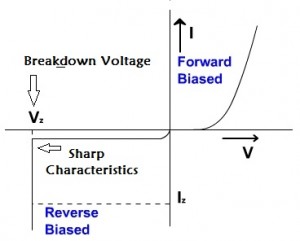
Ideal Zener Diode:
For an ideal Zener diode in the VI graph the breakdown region is considered to be vertical. This shows that the voltage is constant even if the current changes. Therefore, the Zener resistance is neglected. Thus, a Zener diode operating in the breakdown region ideally acts like a battery.
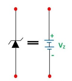
In a circuit, an ideal Zener diode can be replaced by a voltage source Vz, when the Zener diode is operating in the breakdown region.
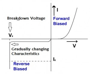
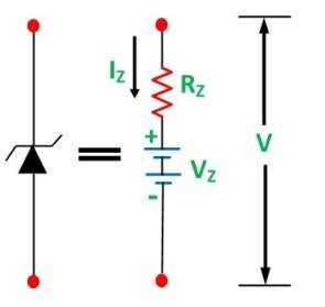
Actual Zener Diode:
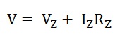
For an actual Zener diode in the V-I graph the breakdown region is not quite vertical. It shows that a Zener diode has a resistance. Hence, an actual Zener diode is considered as a resistance Rz connected in series with a battery of voltage Vz as shown in the figure below.
The voltage across the Zener diode will be