P-N Junction:
P-N junction diode is the most fundamental and the simplest electronics device. When one side of an intrinsic semiconductor is doped with acceptor i.e, one side is made p-type by doping with n-type material, a p-n junction diode is formed.
Capacitance of P-N Junction Diode:
Any variation of the charge within a p-n diode with an applied voltage variation yields a capacitance which must be added to the circuit model of a p-n diode. The capacitance associated with the charge variation in the depletion layer is called the junction capacitance, while the capacitance associated with the excess carriers in the quasi-neutral region is called the diffusion capacitance.
Expressions for the capacitances are obtained by calculating the change in charge for a change in applied voltage, or:

Types of Capacitance of P-N Junction Diode:
In a p-n junction diode, two types of capacitance take place. They are,
- Transition capacitance (CT)
- Diffusion capacitance (CD)
Transition capacitance (CT):
The conducting plates or electrodes of the capacitor are good conductors of electricity. Therefore, they easily allow electric current through them. On the other hand, dielectric material or medium is poor conductor of electricity. Therefore, it does not allow electric current through it. However, it efficiently allows electric field.
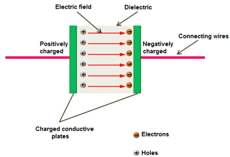
When voltage is applied to the capacitor, charge carriers starts flowing through the conducting wire. When these charge carriers reach the electrodes of the capacitor, they experience a strong opposition from the dielectric or insulating material. As a result, a large number of charge carriers are trapped at the electrodes of the capacitor. These charge carriers cannot move between the plates. However, they exerts electric field between the plates. The charge carriers which are trapped near the dielectric material will stores electric charge. The ability of the material to store electric charge is called capacitance.
In a reverse biased p-n junction diode, the p-type and n-type regions have low resistance. Hence, p-type and n-type regions act like the electrodes or conducting plates of the capacitor. The depletion region of the p-n junction diode has high resistance. Hence, the depletion region acts like the dielectric or insulating material. Thus, p-n junction diode can be considered as a parallel plate capacitor.
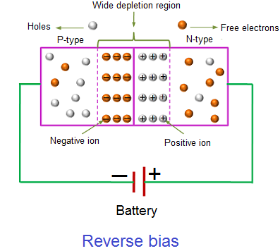
The amount of capacitance changed with increase in voltage is called transition capacitance. The transition capacitance is also known as depletion region capacitance, junction capacitance or barrier capacitance. Transition capacitance is denoted as CT.
The change of capacitance at the depletion region can be defined as the change in electric charge per change in voltage.
CT = dQ / dV
Where,
CT = Transition capacitance
dQ = Change in electric charge
dV = Change in voltage
The transition capacitance can be mathematically written as,
CT = ε A / W
Where,
ε = Permittivity of the semiconductor
A = Area of plates or p-type and n-type regions
W = Width of depletion region
Diffusion capacitance (CD):
Diffusion capacitance occurs in a forward biased p-n junction diode. Diffusion capacitance is also sometimes referred as storage capacitance. It is denoted as CD.
In a forward biased diode, diffusion capacitance is much larger than the transition capacitance. Hence, diffusion capacitance is considered in forward biased diode.
When forward bias voltage is applied to the p-n junction diode, electrons (majority carriers) in the n-region will move into the p-region and recombines with the holes. In the similar way, holes in the p-region will move into the n-region and recombines with electrons. As a result, the width of depletion region decreases.
The electrons (majority carriers) which cross the depletion region and enter into the p-region will become minority carriers of the p-region similarly; the holes (majority carriers) which cross the depletion region and enter into the n-region will become minority carriers of the n-region.
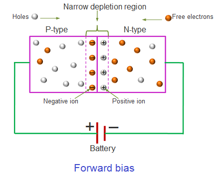
When the width of depletion region decreases, the diffusion capacitance increases. The diffusion capacitance value will be in the range of nano farads (nF) to micro farads (μF).
The formula for diffusion capacitance is
CD = dQ / dV
Where,
CD = Diffusion capacitance
dQ = Change in number of minority carriers stored outside the depletion region
dV = Change in voltage applied across diode

Very nice .There are so easy and so using daily word