The Common-collector Amplifier:
A common collector amplifier (also known as an emitter follower) is one of three basic single-stage bipolar junction transistor (BJT) amplifier topologies, typically used as a voltage buffer.
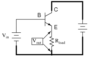
In this circuit the base terminal of the transistor serves as the input, the emitter is the output, and the collector is common to both (for example, it may be tied to ground reference or a power supply rail), hence its name. The analogous field-effect transistor circuit is the common drain amplifier and the analogous tube circuit is the cathode follower.
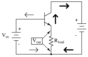
It is called the common-collector configuration because (ignoring the power supply battery) both the signal source and the load share the collector lead as a common connection point as in Figure below.
It should be apparent that the load resistor in the common-collector amplifier circuit receives both the base and collector currents, being placed in series with the emitter. Since the emitter lead of a transistor is the one handling the most current (the sum of base and collector currents, since base and collector currents always mesh together to form the emitter current), it would be reasonable to presume that this amplifier will have a very large current gain. This presumption is indeed correct: the current gain for a common-collector amplifier is quite large, larger than any other transistor amplifier configuration. However, this is not necessarily what sets it apart from other amplifier designs.
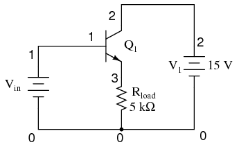
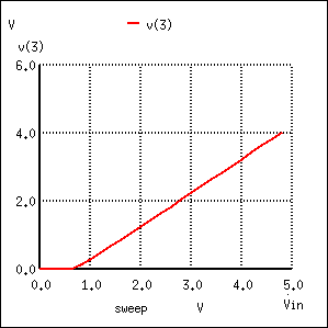
Let’s proceed immediately to a SPICE analysis of this amplifier circuit, and you will be able to immediately see what is unique about this amplifier. The circuit is in Figure below.
Input Characteristics of Common-collector Amplifier:
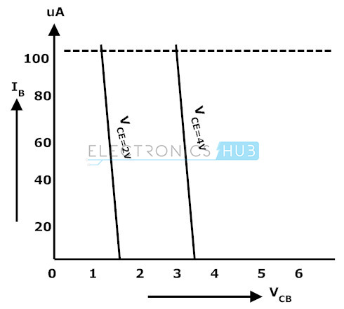
The input characteristics of a common collector configuration are quite different from the common base and common emitter configurations because the input voltage VBC is largely determined by VEC level. Here,
The input characteristics of a common-collector configuration are obtained between inputs current IB and the input voltage VCB at constant output voltage VEC. Keep the output voltage VEC constant at different levels and vary the input voltage VBC for different points and record the IB values for each point. Now using these values we need to draw a graph between the parameters of VBC and IB at constant VEC.
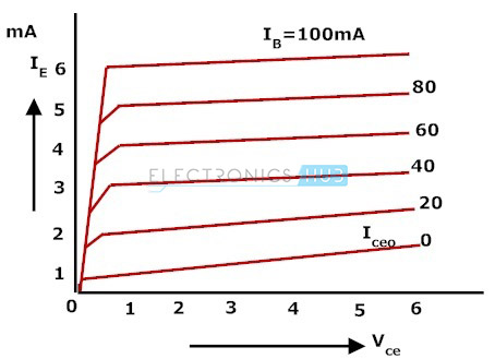
Output Characteristics of Common-collector Amplifier:
The operation of the common collector circuit is same as that of common emitter circuit. The output characteristics of a common collector circuit are obtained between the output voltage VEC and output current IE at constant input current IB. In the operation of common collector circuit if the base current is zero then the emitter current also becomes zero. As a result no current flows through the transistor
If the base current increases then the transistor operates in active region and finally reaches to saturation region. To plot the graph first we keep the IB at constant value and we will vary the VEC value for various points, now we need to record the value of IE for each point. Repeat the same process for different IB values. Now using these values we need to plot the graph between the parameters of IE and VCE at constant values of IB. The below figure show the output characteristics of common collector.