What is Transistor Biasing:
Transistor Biasing is the process of setting a transistors DC operating voltage or current conditions to the correct level so that any AC input signal can be amplified correctly by the transistor.
Transistor Biasing:
Establishing the correct operating point requires the proper selection of bias resistors and load resistors to provide the appropriate input current and collector voltage conditions. The correct biasing point for a bipolar transistor, either NPN or PNP, generally lies somewhere between the two extremes of operation with respect to it being either “fully-ON” or “fully-OFF” along its load line. This central operating point is called the “Quiescent Operating Point”, or Q-point for short.
When a bipolar transistor is biased so that the Q-point is near the middle of its operating range, that is approximately halfway between cut-off and saturation, it is said to be operating as a Class-A amplifier.
This mode of operation allows the output current to increase and decrease around the amplifiers Q-point without distortion as the input signal swings through a complete cycle. In other words, the output current flows for the full 360o of the input cycle.
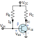
Transistor Biasing with Emitter Feedback:
This type of transistor biasing configuration, often called self-emitter biasing, uses both emitter and collector-base feedback to stabilize the collector current even more as resistors RB and RE as well as the emitter-base junction of the transistor are all effectively connected in series with the supply voltage, VCC.
The downside of this emitter feedback configuration is that the output has reduced gain because of the base resistor connection as the collector voltage determines the current flowing through the feedback resistor, RB producing what is called “degenerative feedback”.
The current flowing from the emitter, IE (which is a combination of IC + :IB) causes a voltage drop to appear across RE in such a direction, that it forward biases the emitter-base junction.
So if the emitter current increases, voltage drop IRE also increases. Since the polarity of this voltage reverse biases the emitter-base junction, IB automatically decrease. Therefore the emitter current increase less than it would have done had there been no self-biasing resistor.
Resistor values are generally set so that the voltage drop across emitter resistor RE is approximately 10% of VCC and the current flowing through resistor RB1 is 10% of the collector current IC.
This type of transistor biasing configuration works best at relatively low power supply voltages.
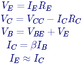
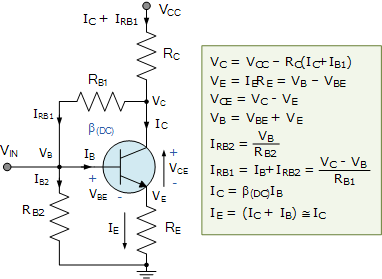
In this circuit, the mathematical equations for different voltages and current are given as