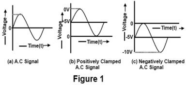
What is Clamping Circuit:
A clamping circuit is used to place either the positive or negative peak of a signal at a desired level. The dc component is simply added or subtracted to/from the input signal. The clamper is also referred to as an IC restorer and AC signal level shifter.
Diode Clampers:
A circuit that places either the positive or negative peak of a signal at a desired D.C level is known as a clamping circuit. A clamping circuit introduces (or restores) a D.C level to an A.C signal. Thus a clamping circuit is also known as D.C restorer, or D.C reinserted or a baseline stabilizer. The following are two general types of clamping.
- Positive clamping occurs when negative peaks raised or clamped to ground or on the zero level
In other words, it pushes the signal upwards so that negative peaks fall on the zero level. - Negative clamping occurs when positive peaks raised or clamped to ground or on the zero level
In other words, it pushes the signal downwards so that the positive peaks fall on the zero level.
In both cases the shape of the original signal has not changed, only there is vertical shift in the signal
Fig. 1 shows the clamping wave- form.
Types of Clampers:
1-POSITIVE CLAMPER:
Fig 2 shows the circuit of a positive clamper It consists of a diode and a capacitor the clamper output
is taken across the load resistance R.
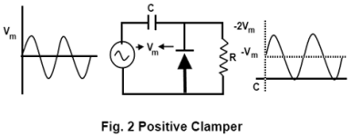
During the negative half-cycle of the input voltage, the diode conducts heavily and behaves as a closed switch At the negative peak, the capacitor is charged to maximum voltage V slightly beyond the negative peak, the diode is shut- off and the capacitor charged to Vm behaves as a battery during the positive half cycle of the input signal. The diode is reversed biased and the output voltage will be equal to Vm + V this gives positive clamped voltage and is called positive clamper circuit.
Positive clamper with bias:
Biased clamper circuit operates in exactly the same manner as unbiased clampers. The different is only that a dc bias voltage is add in series with the diode and resistor. A biased clamper means that the clamping can be done at any voltage level other than zero.
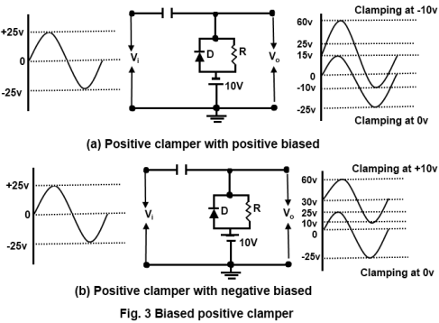
Fig 3(a) shows the circuit of positive clamper with positive biased Here a battery of 10 V is added in such a way that the clamping take place positively at 10V. Similarly, it is possible to clamp the input wave form positively at 10V
by reversing the battery connections as shown in Fig 3(b).
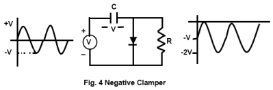
NEGATIVE CLAMPER:
Fig 4 shows the circuit of a negative clamper during the positive half cycle of the input signal, the capacitor is charged to Vm, with the polarity shown in Fig 4. Observe that voltage across the capacitor is opposing the input voltage V. This gives negative clamped voltage and is called negative clamper circuit.
Negative Clamper With bias:
Fig 5 (a) shows the circuit of negative clamper with positive bias. With no input signal the capacitor charges to the battery voltage and the output is positive because the negative side of the batter is grounded. The output waveform is clamped to +10V, the value of the battery. Since this is a negative clamper (cathode to ground), the top of the output wave touch the +10V reference line.
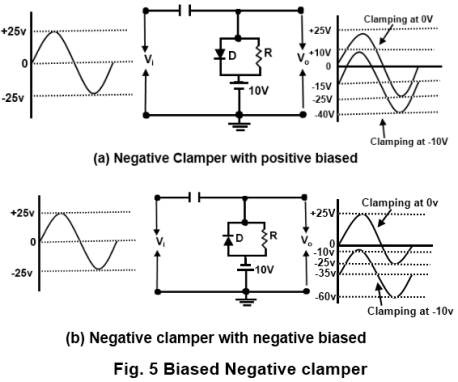
Similarly, it is possible to clamp the input waveform negatively at by reversing the battery connections as shown in Fig 5(b)
ASYNCHRONOUS AND SYNCHRONOUS CLAMPING:
Clamping circuit discussed above are examples of clamping circuit in which the time during which the clamping is effective is controlled by the signal itself is called non-synchronous or Asynchronous On the other hand, When the time of clamping is not determined directly by the signal but is determined rather by an auxiliary voltage. Such circuits are called synchronous clamping circuit.
For example, suppose the wave- form of Fig 6(a) is to be used to displace the beam of a cathode ray tube linearly with time, first in one direction and then in other direction from some fixed initial point. If the signal is transmitted through an ac coupling network whose. low frequency time constant is not very large in comparison with the time interval T1, signal will distort as shown in Fig, 6 (b). The cause defect in the waveform is that the two displacements will start for different point A and B Also the d c level VR is
lost.
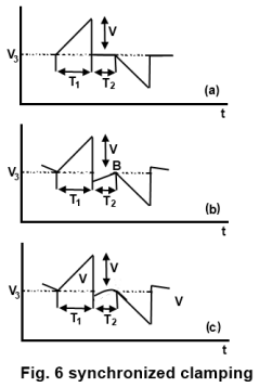
If however, the signal is passed through the circuit of Fig 7 and if switch S is closed during time interval T2 and is open during time T1, the wave- form will receive as in Fig 6(c) The pips which appear when the voltage returns to the level R will be reduced to’ infinitesimally narrow spikes as the resistance of the switch Rf approaches zero.
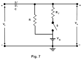
It is needed that the switch S be open throughout the time interval T1, but it is not necessary that thy switch be closed off the entire interval T2. It is only needed that the switch be closed for a period long enough to allow the capacitor C to acquire or lose enough charge to bring the output terminal to the reference level VR.

Sir Thanku Verry Much For This Valuable Content