MOSFET (Metal Oxide Semiconductor Field Effect Transistor):
MOSFETS conduct through a conductive region or path called “the channel”. We can make this conductive channel wider or smaller by applying a suitable gate potential. An electric field induced around the gate terminal by the application of this gate voltage affects the electrical characteristics of the channel, thus the name field-effect transistor.
Types of MOSFET:
P-Channel MOSFET:
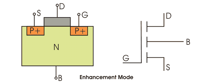
MOSFET which has p – channel region between source any gate is known as p – channel MOSFET. It is a four terminal devices, the terminals are gate, drain, source and substrate or body. The drain and source are heavily doped p+ region and the substrate is in n-type. The current flows due to the flow of positively charged holes that’s why it is known as p-channel MOSFET.
When we apply negative gate voltage, the electrons present beneath the oxide layer, experiences repulsive force and they are pushed downward in to the substrate, the depletion region is populated by the bound positive charges which are associated with the donor atoms. The negative gate voltage also attracts holes from p+ source and drain region in to the channel region. Thus hole which channel is formed now if a voltage between the source and the drain is applied current flows.
The gate voltage controls the hole concentration of the channel. The diagram of p- channel enhancement and depletion MOSFET are given below.
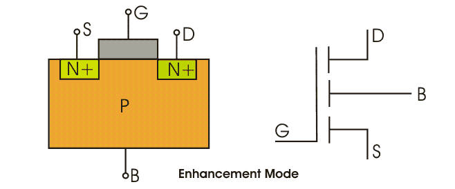
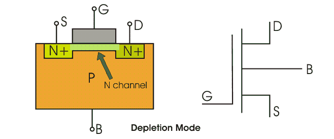
N-Channel MOSFET:
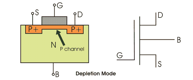
MOSFET having n-channel region between source and drain is known as n-channel MOSFET . It is a four terminal device, the terminals are gate, drain and source and substrate or body. The drain and source are heavily doped n+ region and the substrate is p-type. The current flows due to flow of the negatively charged electrons, that’s why it is known as n- channel MOSFET.
When we apply the positive gate voltage the holes present beneath the oxide layer experiences repulsive force and the holes are pushed downwards in to the bound negative charges which are associated with the acceptor atoms. The positive gate voltage also attracts electrons from n+ source and drain region in to the channel thus an electron reach channel is formed, now if a voltage is applied between the source and drain. The gate voltage controls the electron concentration in the channel n-channel MOSFET is preferred over p-channel MOSFET as the mobility of electrons are higher than holes.
The diagrams of enhancements mode and depletion mode are given below.
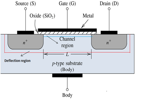
Working Principle of MOSFET:
The working principle of MOSFET depends up on the MOS capacitor. The MOS capacitor is the main part. The semiconductor surface at below the oxide layer and between the drain and source terminal can be inverted from p-type to n-type by applying a positive or negative gate voltages respectively. When we apply positive gate voltage the holes present beneath the oxide layer experience repulsive force and the holes are pushed downward with the substrate.
The depletion region is populated by the bound negative charges, which are associated with the acceptor atoms. The positive voltage also attracts electrons from the n+ source and drain regions in to the channel. The electron reach channel is formed.
Now, if a voltage is applied between the source and the drain, current flows freely between the source and drain gate voltage controls the electrons concentration the channel. Instead of positive if apply negative voltage a hole channel will be formed beneath the oxide layer.