Bipolar Junction Transistor (BJT):
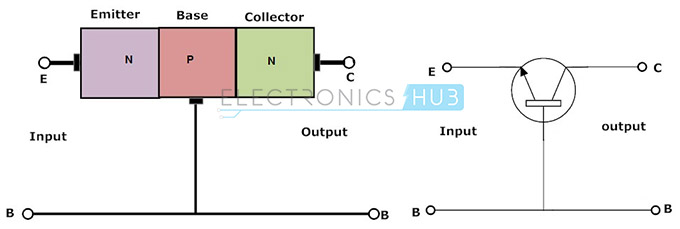
A Bipolar Junction Transistor (BJT) has three terminals connected to three doped semiconductor regions. In an N-P-N transistor, a thin and lightly doped P-type base is sandwiched between a heavily doped N-type emitter and another N-type collector; while in a P-N-P transistor, a thin and lightly doped N-type base is sandwiched between a heavily doped P-type emitter and another P-type collector. In the following, we will only consider NPN BJTs.
Bipolar Junction Transistors Characteristics:
The three parts of a BJT are collector, emitter and base. Before knowing about the bipolar junction transistor characteristics, we have to know about the modes of operation for this type of transistors. The modes are
- Common Base (CB) mode
- Common Emitter (CE) mode
- Common Collector (CC) mode
Common Base Characteristics:
In this configuration, we use base as common terminal for both input and output signals. Here the input is applied between the base and emitter terminals and the corresponding output signal is taken between the base and collector terminals with the base terminal grounded. Here the input parameters are VEB and IE and the output parameters are VCB and IC. The input current flowing into the emitter terminal must be higher than the base current and collector current to operate the transistor, therefore the output collector current is less than the input emitter current.
This transistor configuration has high output impedance and low input impedance. This type of configuration has high resistance gain i.e. ratio of output resistance to input resistance is high. The voltage gain for this configuration of circuit is given below.
AV = Vout/Vin = (IC*RL) / (IE*Rin)
Current gain in common base configuration is given as
α = Output current/Input current
α = IC/IE
The common base circuit is mainly used in single stage amplifier circuits, such as microphone pre amplifier or radio frequency amplifiers because of their high-frequency response. The common base transistor circuit is given below.
Input Characteristics:
For p-n-p transistor, the input current is the emitter current (IE) and the input voltage is the collector base voltage (VCB).
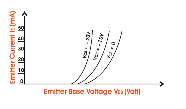
As the emitter – base junction is forward biased, therefore the graph of IE Vs VEB is similar to the forward characteristics of a p – n diode. IE increases for fixed VEB when VCB increases.
Output Characteristics:
The output characteristics show the relation between output voltage and output current IC is the output current and collector-base voltage and the emitter current IE is the input current and works as the parameters.
The figure below shows the output characteristics for a p-n-p transistor in CB mode.
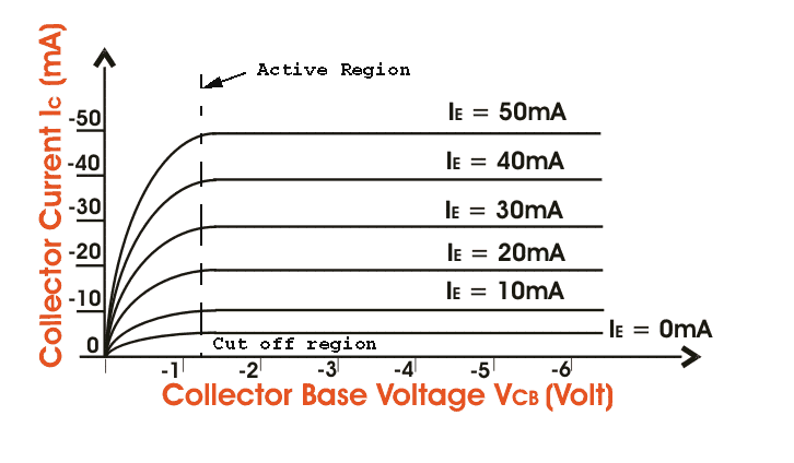
As we know for p-n-p transistors IE and VEB are positive and IC, IB, VCB are negative. These are three regions in the curve, active region saturation region and the cut off region. The active region is the region where the transistor operates normally. Here the emitter junction is reverse biased.
