Common Source JFET Amplifier:
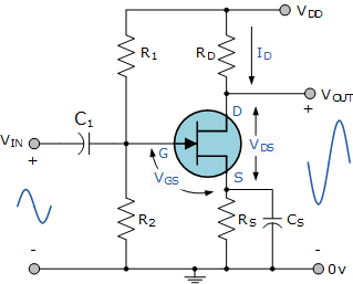
The amplifier circuit consists of an N-channel JFET, but the device could also be an equivalent N-channel depletion-mode MOSFET as the circuit diagram would be the same just a change in the FET, connected in a common source configuration. The JFET gate voltage Vg is biased through the potential divider network set up by resistors R1 and R2 and is biased to operate within its saturation region which is equivalent to the active region of the bipolar junction transistor.
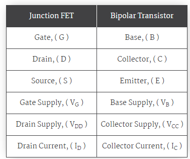
Unlike a bipolar transistor circuit, the junction FET takes virtually no input gate current allowing the gate to be treated as an open circuit. Then no input characteristics curves are required. We can compare the JFET to the bipolar junction transistor (BJT) in the following table’
JFET to BJT Comparison
Since the N-Channel JFET is a depletion mode device and is normally “ON”, a negative gate voltage with respect to the source is required to modulate or control the drain current. This negative voltage can be provided by biasing from a separate power supply voltage or by a self biasing arrangement as long as a steady current flows through the JFET even when there is no input signal present and Vg maintains a reverse bias of the gate-source pn junction.
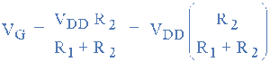
In our simple example, the biasing is provided from a potential divider network allowing the input signal to produce a voltage fall at the gate as well as voltage rise at the gate with a sinusoidal signal. Any suitable pair of resistor values in the correct proportions would produce the correct biasing voltage so the DC gate biasing voltage Vg is given as:
The efficiency of the common source JFET amplifier can be improved by the addition of a resistor, Rs included in the source lead with the same drain current flowing through this resistor. Resistor, Rs is also used to set the JFET amplifiers “Q-point”.
When the JFET is switched fully “ON” a voltage drop equal to Rs x Id is developed across this resistor raising the potential of the source terminal above 0v or ground level. This voltage drop across Rs due to the drain current provides the necessary reverse biasing condition across the gate resistor, R2 effectively generating negative feedback.
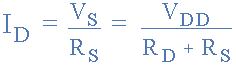
So in order to keep the gate-source junction reverse biased, the source voltage, Vs needs to be higher than the gate voltage, Vg. This source voltage is therefore given as:
![]()
Then the Drain current, Id is also equal to the Source current, Is as “No Current” enters the Gate terminal and this can be given as:
Common Source JFET Amplifier Characteristics Curves:

As with the common emitter bipolar circuit, the DC load line for the common source JFET amplifier produces a straight line equation whose gradient is given as: -1/(Rd + Rs) and that it crosses the vertical Id axis at point A equal to Vdd/(Rd + Rs). The other end of the load line crosses the horizontal axis at point B which is equal to the supply voltage, Vdd.
The actual position of the Q-point on the DC load line is generally positioned at the mid center point of the load line (for class-A operation) and is determined by the mean value of Vg which is biased negatively as the JFET is a depletion-mode device. Like the bipolar common emitter amplifier the output of the Common Source JFET Amplifier is 180o out of phase with the input signal.
