Characteristics of JFETS:
There are two types of static characteristics viz
(1) Output or drain characteristic and
(2) Transfer characteristic.
Output or Drain Characteristic:
The curve drawn between drain current Ip and drain-source voltage VDS with gate-to-source voltage VGS as the parameter is called the drain or output characteristic. This characteristic is analogous to collector characteristic of a BJT:
(a) Drain Characteristic With Shorted-Gate. The circuit diagram for determining the drain characteristic with shorted-gate for an N-channel JFET is given in figure. and the drain characteristic with shorted-gate is shown in another figure.
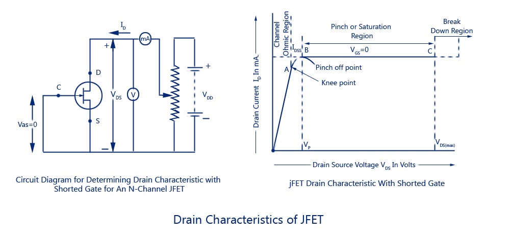
Initially when drain-source voltage Vns is zero, there is no attracting potential at the drain, so no current flows inspite of the fact that the channel is fully open. This gives drain current Ip = 0. For small applied voltage Vna, the N-type bar acts as a simple semiconductor resistor, and the drain current increases linearly with_the increase in Vds, upto the knee point. This region, (to the left of the knee point) of the curve is called the channel ohmic region, because in this region the FET behaves like an ordinary resistor.
It is to be noted that in the pinch-off (or saturation) region the channel resistance increases in proportion to increase in VDS and so keeps the drain current almost constant and the reverse bias required by the gate-channel junction is supplied entirely by the voltage drop across the channel resistance due to flow of IDsg and not by the external bias because VGS = 0
Drain current in the pinch of region is given by Shockley’s equation
where ID is the drain current at a given gate-source voltage VGS, IDSS is the drain-current with gate shorted to source and VGS (0FF) is the gate-source cut-off voltage.
If drain-source voltage, Vds is continuously increased, a stage comes when the gate-channel junction breaks down. At this point current increases very rapidly. and the JFET may be destroyed. This happens because the charge carriers making up the saturation current at the gate-channel junction accelerate to a high velocity and produce an avalanche effect.
Drain Characteristics With External Bias:
The circuit diagram for determining the drain characteristics with different values of external bias is shown in figure. and a family of drain characteristics for different values of gate-source voltage VGS is given in next figure
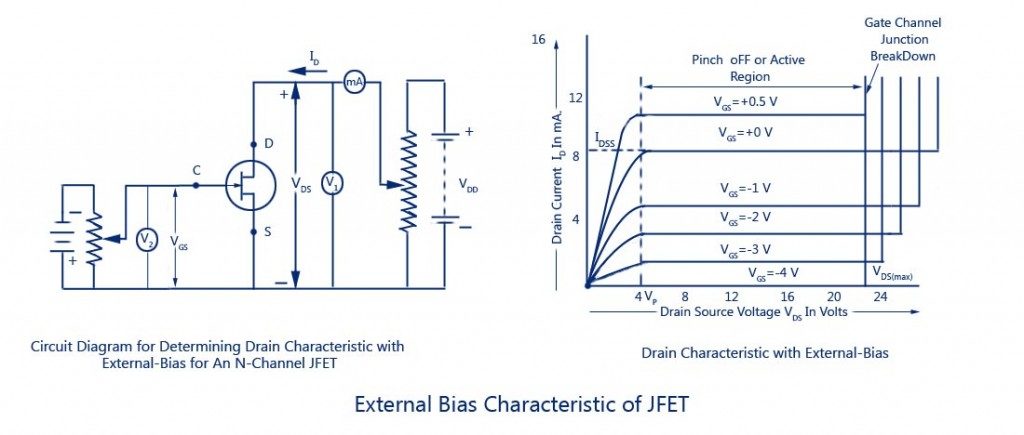
It is observed that as the negative gate bias voltage is increased
(1) The maximum saturation drain current becomes smaller because the conducting channel now becomes narrower.
(2) Pinch-off voltage is reached at a lower value of drain current ID than when VGS = 0. When an external bias of, say – 1 V is applied between the gate and the source, the gate-channel junctions are reverse-biased even when drain current, ID is zero. Hence the depletion regions are already penetrating the channel to a certain extent when drain-| source voltage, VDS is zero. Due to this reason, a smaller voltage drop along the channel (i.e. smaller than that for VGS = 0) will increase the depletion regions to the point where 1 they pinch-off the current. Consequently, the pinch-off voltage VP is reached at a lower 1 drain current, ID when VGS = 0.
(3) The ohmic region portion decreases.
(4) Value of drain-source voltage VDS for the avalanche breakdown of the gate junction is reduced.
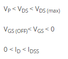
Hence for working of JFET in the pinch-off or active region it is necessary that the following conditions be fulfilled.
2. Transfer Characteristic of JFET:
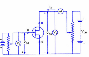
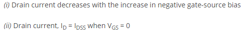
The transfer characteristic for a JFET can be determined experimentally, keeping drain-source voltage, VDS constant and determining drain current, ID for various values of gate-source voltage, VGS. The circuit diagram is shown in fig. 9.7 (a). The curve is plotted between gate-source voltage, VGS and drain current, ID, as illustrated in fig. 9.8. It is similar to the transconductance characteristic of a vacuum tube or a transistor. It is observed that
![]()
![]()
The transfer characteristic can also be derived from the drain characteristic by noting values of drain current, IDcorresponding to various values of gate-source voltage, VGS for a constant drain-source voltage and plotting them.
It may be noted that a P-channel JFET operates in the same way and have the similar characteristics as an N-channel JFET except that channel carriers are holes instead of electrons and the polarities of VGS and VDS are reversed.
