JFET or Junction Field Effect Transistor:
The junction field effect transistor or JFET is one of the simplest transistors from the structural point of view. It is a voltage controlled semiconductor device. In this, the current is carried by only one type of carriers. So, it is a unipolar device. It has a very high input electrical resistance.
Construction of JFETs:
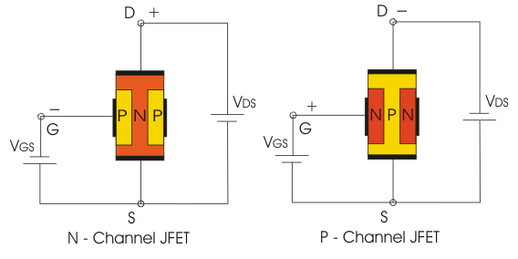
JFET consists of a doped Si or GaAs bar. There are ohmic contacts, the two ends of the bar and semiconductor junction on its two sides. If the semiconductor bar is n-type, the two sides of the bar is heavily doped with p – type impurities and this is known as n – channel JFET.
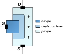
On the other hand if the semiconductor bar is p- type, the two sides of the bar is heavily doped with n – type impurities and this is known as p- channel JFET. When a voltage is applied between the two ends, a current which is carried by the majority carriers of the bar flows along the length of the bar. There are several terminals in JFET. The terminal through which the majority carrier enter the bar and the terminal through which they leave are known as source (s) and drain (D) respectively. The heavily doped region on the two sides is known as the gate (G).
There are several terminals in JFET. The terminal through which the majority carrier enter the bar and the terminal through which they leave are known as source (s) and drain (D) respectively. The heavily doped region on the two sides is known as the gate (G). In junction field effect transistor, the junction is a reverse biased. As a result, depletion regions form, which extend to the bar. By changing gate to source voltage, the depletion width can be controlled. So, the effective cross section area decreased with increasing reverse bias. So, the drain current is a function of the gate to the source voltage:
By changing gate to source voltage, the depletion width can be controlled. So, the effective cross section area decreased with increasing reverse bias. So, the drain current is a function of the gate to the source voltage.
N-Channel JFET:
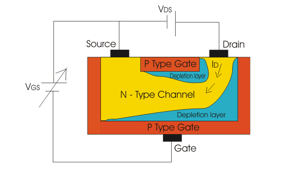
A semiconductor bar of n-type material is taken & ohmic contacts are made on either ends of the bar. Terminals are brought out from these ohmic contacts and named as drain & source as shown in the figure below. On the other two sides of the n-type semiconductor bar, heavily doped p-type regions are formed to create a p-n junction. Both these p-type regions are connected together via ohmic contacts and the gate terminal is brought out as seen below.
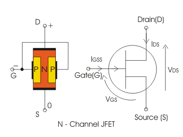
Figure shows the n-channel and p-channel JFET with symbols. The arrow on the gate indicates the direction of the current. Current flows through the length of the n-type bar (channel) due to majority charge carries which in this case are electrons. When a voltage is applied between the two ends, a current which is carried by the majority carriers electrons flows along the length of a bar. The majority carriers enter the bar through the source terminal and leave through the drain terminal. The heavily doped regions of the n-type bar are known as the gates. The
The majority carriers enter the bar through the source terminal and leave through the drain terminal. The heavily doped regions of the n-type bar are known as the gates. The gate-source junctions is reverse is biased as a result depletion regions from which extend to the bar by changing gate to source voltage effective cross-sectional area decreases with the function of the gate to source voltage.
P-Channel JEFT:
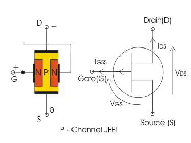
p-channel JFET consists of a p-type silicon or GaAs. Two sides of the bar is heavily doped with n-type impurities. When a voltage is applied between the two ends, a current which is carried by the majority carrier holes flow along the length of a bar. The gate source junction is reverse biased as a result depletion regions form, which extend to the bar by changing gate to extend to source voltage the depletion width can be controlled. The effective cross sectional area decreased with increasing reverse bias, so the drain current is the function of the gate to source voltage.
Biasing of JFET:
The gate to source p-n junction of a JFET is always reverse biased and supply voltage is given across the drain to source terminal.
Operation of Junction Field Effect Transistor or JFET:
Operation with gate to source voltage = 0
If an n-channel JFET is biased as explained above and the gate to source voltage is kept zero, due to the positive drain to source voltage few electrons which are available for conduction in the n-type material will start flowing from the narrow passage (channel) from source to drain. This current is called as drain current. As the channel has some finite resistance it will cause some voltage drop across the channel. Hence the depletion region of the p-n junction starts increasing and penetrates more into the n-type material as it is lightly doped. Due to this the width of the channel available for conduction is reduced. The penetration of the depletion region into the n-type region depends on the reverse bias voltage. Maximum drain current ID(MAX) will flow through the device when the channel is widest i.e. when VGS is zero.
Operation with negative gate to source voltage As a negative voltage is applied to the gate to source p-n junction the depletion region increases and penetration of the depletion region into the n-type channel further increases. If the negative gate to source voltage is further increased the depletion region spreads more and more inside the n-type bar. Due to this less and less number of charge carries (electrons) can pass through the channel and the drain current reduces. Hence, with increase in negative gate to source voltage drain current reduces. At a certain value of this voltage the depletion region from both the ends will increase and touch each other and the drain current will become zero. This gate to source voltage at which drain current is cut off is called as VGS(OFF). As seen the VGS controls ID. Hence, JFET is a voltage controlled device. The relationship between ID and VGS is given by Shockley’s equation
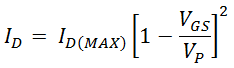
Where, VP is the pinch-off voltage which is the value of drain to source VDS at which drain current reaches its constant saturation value. Any further increase in VDS does not affect ID.
Junction Field Effect Transistor Characteristics:
In this characteristics we can find three regions,
-
The linear or the ohmic region:
Here the drain to source voltage is small and drain current in nearly proportional to the drain to source voltage. When a positive drain to source voltage is applied, this voltage increases from zero to a small value, the depletion region width remain very small and under this condition the semi conductor bar behaves just like a resistor. So, drain current increases almost linearly with drain to source voltage.
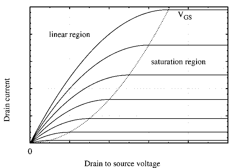
2. The saturation of the active region:
Here the drain current is almost constant and it is not dependent on the drain to source voltage actually. When the drain to source voltage continuous to increase the channel resistance increases and at some point, the depletion regions meet near the drain to pinch off the channel. Beyond that pinch off voltage, the drain, current attains saturation.
3. The breakdown voltage:
Here the drain current increases rapidly with a small increase of the drain to source voltage. Actually for large value of drain to source voltage, a breakdown of the gate junction takes place which results a sharp increase of the drain current.
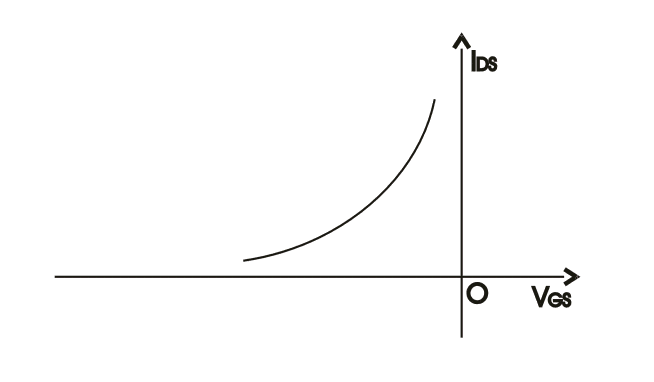
Transfer characteristics:
The graphical characteristics plot of the saturation drain current against the gate to source voltage is known as the transfer characteristics of JFET. It can be obtained from static characteristics very easily. The transfer characteristics of an n- channel is shown below