Introduction to MOSFET:
The metal–oxide–semiconductor field-effect transistor (MOSFET) is a transistor used for amplifying or switching electronic signals. In MOSFETs, a voltage on the oxide-insulated gate electrode can induce a conducting channel between the two other contacts called source and drain. The channel can be of n-type or p-type, and is accordingly called an nMOSFET or a pMOSFET. Figure 1 shows the schematic diagram of the structure of an nMOS device before and after channel formation.
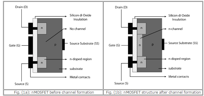
Figure 2, shows symbols commonly used for MOSFETs where the bulk terminal is either labeled (B) or implied (not drawn).

Output Characteristics of MOSFET:
MOSFET output characteristics plot ID versus VDS for several values of VGS.
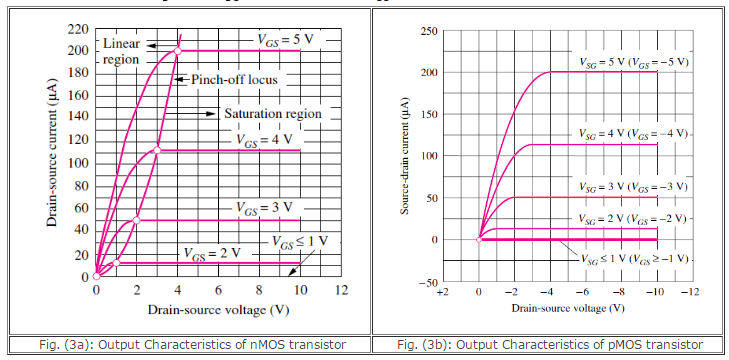
The characteristics of an nMOS transistor can be explained as follows. As the voltage on the top electrode increases further, electrons are attracted to the surface. At a particular voltage level, which we will shortly define as the threshold voltage, the electron density at the surface exceeds the hole density. At this voltage, the surface has inverted from the p-type polarity of the original substrate to an n-type inversion layer, or inversion region, directly underneath the top plate as indicated in Fig. 1(b).
This inversion region is an extremely shallow layer, existing as a charge sheet directly below the gate. In the MOS capacitor, the high density of electrons in the inversion layer is supplied by the electron–hole generation process within the depletion layer. The positive charge on the gate is balanced by the combination of negative charge in the inversion layer plus negative ionic acceptor charge in the depletion layer.
The voltage at which the surface inversion layer just forms plays an extremely important role in field-effect transistors and is called the threshold voltage Vtn. The region of output characteristics where VGS<vtn and no current flows is called the cutt-off region. When the channel forms in the nMOS (pMOS) transistor, a positive (negative) drain voltage with respect to the source creates a horizontal electric field moving the electrons (holes) toward the drain forming a positive (negative) drain current coming into the transistor. The positive current convention is used for electron and hole current, but in both cases electrons are the actual charge carriers. If the channel horizontal electric field is of the same order or smaller than the vertical thin oxide field, then the inversion channel remains almost uniform along the device length.
This continuous carrier profile from drain to source puts the transistor in a bias state that is equivalently called either the non-saturated, linear, or ohmic bias state. The drain and source are effectively short-circuited. This happens when VGS > VDS + Vtn for nMOS transistor and VGS < VDS +Vtp for pMOS transistor. Drain current is linearly related to drain-source voltage over small intervals in the linear bias state.
But if the nMOS drain voltage increases beyond the limit, so that VGS < VDS + Vtn, then the horizontal electric field becomes stronger than the vertical field at the drain end, creating an asymmetry of the channel carrier inversion distribution shown in Figure 4.
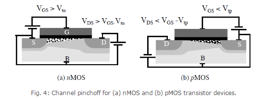
If the drain voltage riseswhile the gate voltage remains the same, then VGD can go below the threshold voltage in the drain region. There can be no carrier inversion at the drain-gate oxide region, so the inverted portion of the channel retracts from the drain, and no longer “touches” this terminal. The pinched-off portion of the channel forms a depletion region with a high electric field.
The n-drain and p-bulk form a pn junction. When this happens the inversion channel is said to be “pinched-off” and the device is in the saturation region. The characteristics can be loosely modelled by the following equations.
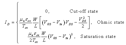
Transfer Characteristics of MOSFET:
The transfer characteristic relates drain current (ID) response to the input gate-source driving voltage (VGS). Since the gate terminal is electrically isolated from the remaining terminals (drain, source, and bulk), the gate current is essentially zero, so that gate current is not part of device characteristics. The transfer characteristic curve can locate the gate voltage at which the transistor passes current and leaves the OFF-state. This is the device threshold voltage (Vtn). Figure 5 shows measured input characteristics for an nMOS and pMOS transistor with a small 0.1V potential across their drain to source terminals.
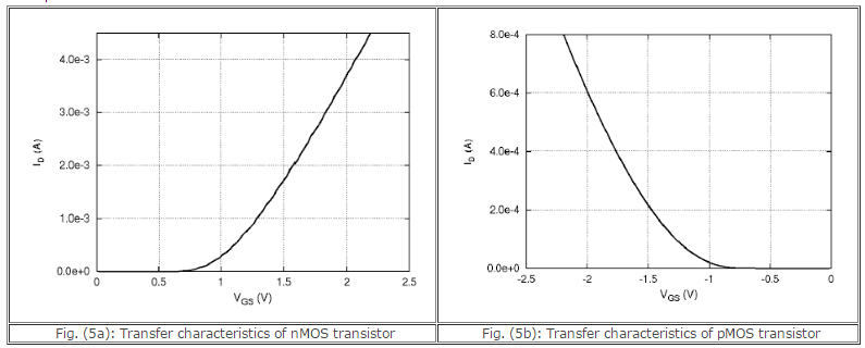
The transistors are in their non-saturated bias states. As VGS increases for the nMOS transistor in Figure 5a, the threshold voltage is reached where drain current elevates. For VGS between 0V and 0.7V, ID is nearly zero indicating that the equivalent resistance between the drain and source terminals is extremely high. Once VGS reaches 0.7V, the current increases rapidly with VGS indicating that the equivalent resistance at the drain decreases with increasing gate-source voltage.
Therefore, the threshold voltage of the given nMOS transistor is about Vtn ≈ 0.7V. The pMOS transistor input characteristic in Figure 5b is analogous to the nMOS transistor except the ID and VGS polarities are reversed.
